前一段有个灵车pm2.5检测器,淘宝只要12块钱。搜了下大概是个放口袋里用蓝牙和手机连接,检测PM2.5浓度的。
搜到了前几年的新闻 -> 传送门
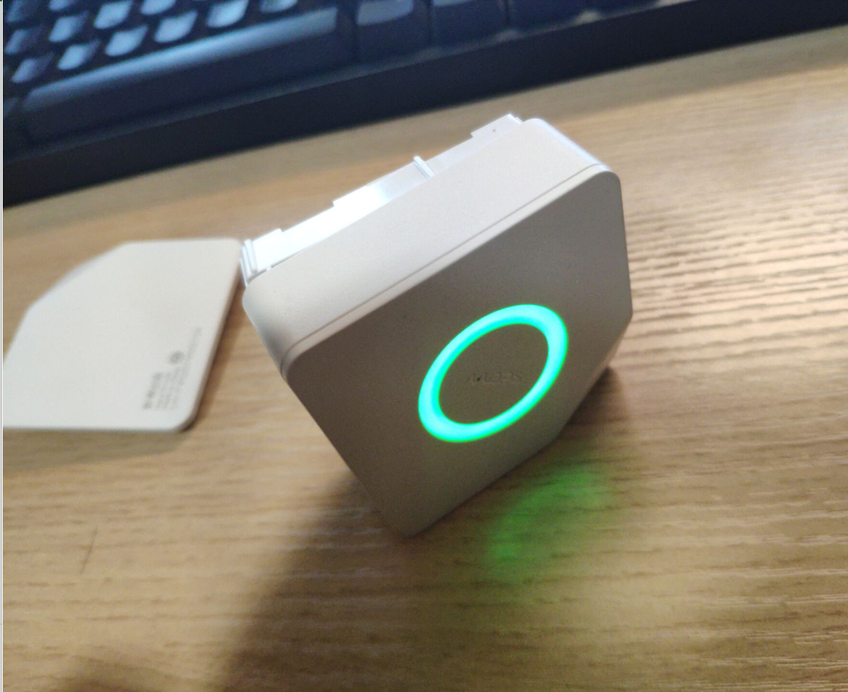
然而买回来才发现,安卓客户端下载链接打不开。估计是厂子跑路了,不然怎么卖这么便宜。于是想自己日了玩玩
0x0 拆了玩玩
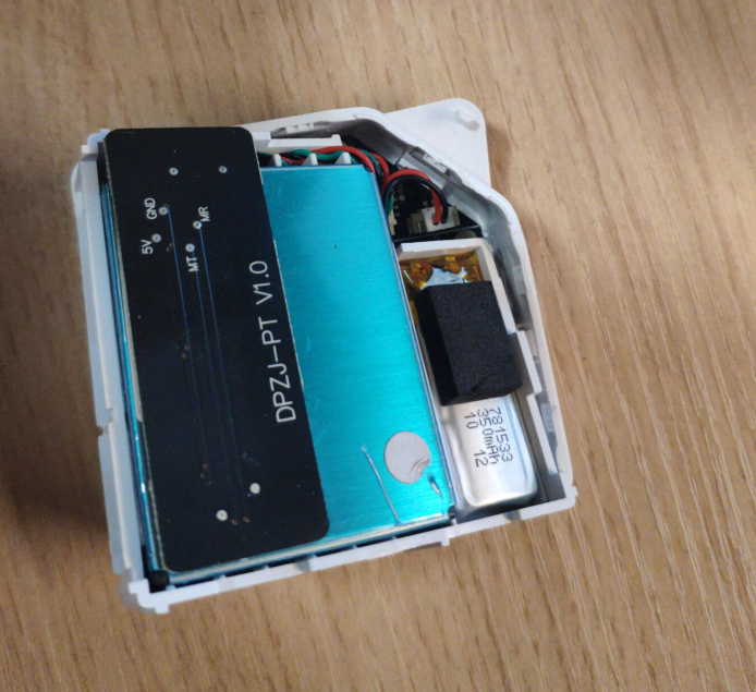
里面很简单一个主板一个PM2.5检测元件一个电池
单片机是nRF51288,一个支持蓝牙的片子
照着数据手册量了一圈发现这里是SWD调试口

从左到右依次是SWCLK,SWIO,GND,?
于是,openocd启动!
然而事情并没有这么简单…
0x1 初次尝试
因为没有客户端,为了能正常用它的PM2.5功能,最简单的方法就是逆一下它的蓝牙通信协议,写个土制客户端。
swd排针是个1.54间距的。。。飞线到洞洞板再插到树莓派上。openocd可以用树莓派的gpio模拟swd或者jtag,不过坑不少。

焊的太丑就不给拍清楚了QAQ,盲猜第四个脚是vcc3.3,顺手接上
openocd的配置文件只有树莓派1和2的,用了cpu频率算一个swd时钟频率,我这个pi3要改一些地方,配置文件改了改如下
#
# Config for using Raspberry Pi's expansion header
#
# This is best used with a fast enough buffer but also
# is suitable for direct connection if the target voltage
# matches RPi's 3.3V and the cable is short enough.
#
# Do not forget the GND connection, pin 6 of the expansion header.
#

interface bcm2835gpio

bcm2835gpio_peripheral_base 0x3F000000

# Transition delay calculation: SPEED_COEFF/khz - SPEED_OFFSET
# These depend on system clock, calibrated for stock 700MHz
# bcm2835gpio_speed SPEED_COEFF SPEED_OFFSET
#bcm2835gpio_speed_coeffs 146203 36
bcm2835gpio_speed_coeffs 194938 48

# Each of the JTAG lines need a gpio number set: tck tms tdi tdo
# Header pin numbers: 23 22 19 21
# bcm2835gpio_jtag_nums 11 25 10 9

# or if you have both connected,
# reset_config trst_and_srst srst_push_pull
reset_config none separate
# Each of the SWD lines need a gpio number set: swclk swdio
# Header pin numbers: 22 18
bcm2835gpio_swd_nums 25 24

# If you define trst or srst, use appropriate reset_config
# Header pin numbers: TRST - 26, SRST - 18

# bcm2835gpio_trst_num 7
# reset_config trst_only

bcm2835gpio_srst_num 18
#reset_config srst_only srst_push_pull

# or if you have both connected,
# reset_config trst_and_srst srst_push_pull

#
# script for Nordic nRF51 series, a Cortex-M0 chip
#

transport select swd
source [find target/swj-dp.tcl]

if { [info exists CHIPNAME] } {
   set _CHIPNAME $CHIPNAME
} else {
   set _CHIPNAME nrf51
}

if { [info exists ENDIAN] } {
   set _ENDIAN $ENDIAN
} else {
   set _ENDIAN little
}

# Work-area is a space in RAM used for flash programming
# By default use 16kB
if { [info exists WORKAREASIZE] } {
   set _WORKAREASIZE $WORKAREASIZE
} else {
   set _WORKAREASIZE 0x4000
}

if { [info exists CPUTAPID] } {
   set _CPUTAPID $CPUTAPID
} else {
   set _CPUTAPID 0x0bb11477
}

swj_newdap $_CHIPNAME cpu -expected-id $_CPUTAPID -irlen 4

set _TARGETNAME $_CHIPNAME.cpu
target create $_TARGETNAME cortex_m -chain-position $_TARGETNAME

$_TARGETNAME configure -work-area-phys 0x20000000 -work-area-size $_WORKAREASIZE -work-area-backup 0

if {![using_hla]} {
   # The chip supports standard ARM/Cortex-M0 SYSRESETREQ signal
   cortex_m reset_config sysresetreq
}

flash bank $_CHIPNAME.flash nrf51 0x00000000 0 1 1 $_TARGETNAME
flash bank $_CHIPNAME.uicr nrf51 0x10001000 0 1 1 $_TARGETNAME

#
#  The chip should start up from internal 16Mhz RC, so setting adapter
#  clock to 1Mhz should be OK
#
adapter_khz 1000

proc enable_all_ram {} {
        # nRF51822 Product Anomaly Notice (PAN) #16 explains that not all RAM banks
        # are reliably enabled after reset on some revisions (contrary to spec.) So after
        # resetting we enable all banks via the RAMON register
        mww 0x40000524 0xF
}
$_TARGETNAME configure -event reset-end {  enable_all_ram }

init
targets
主要改了以下几个地方
-irlen 4// nrf51里面是个32位M0核,指令长度4字节bcm2835gpio_speed_coeffs 194938 48// 树莓派3的cpu频率和2不一样,原来是拿2的配置文件改的reset_config none separate// 没接reset脚,这里让openocd不要管rst信号,不然后面reset会卡住然后超时transport select swd// 神秘问题,不指定swd会默认走jtag然后不让改
然后板子通电,openocd -f xxx.cfg不出意外就可以看到芯片了

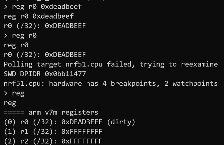
nc连上127.0.0.1:4444进openocd终端,试一下就可以正常调试了
然而问题出在这里
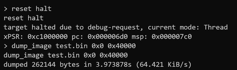
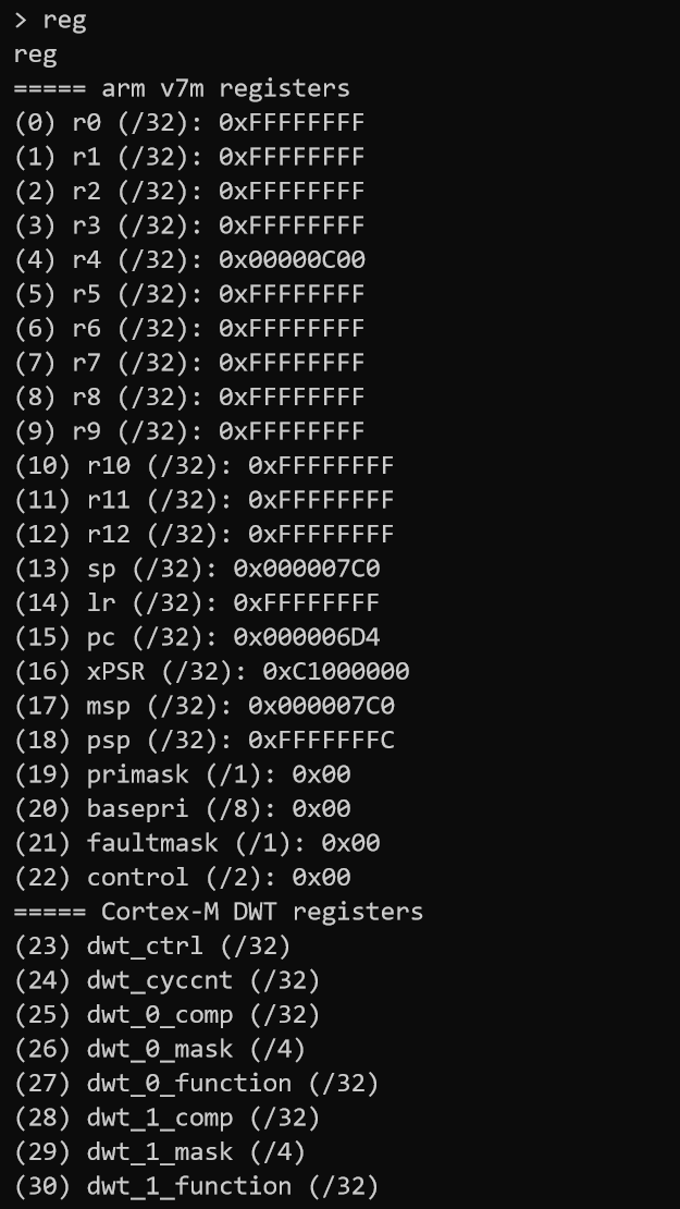
读出来是全0
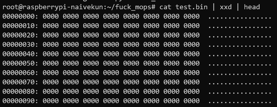
pc指向的代码也读不出来
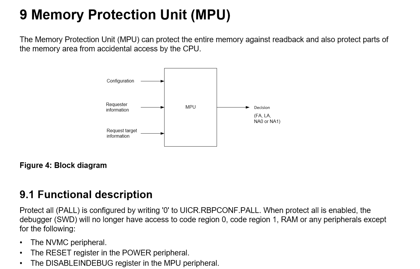
查了下手册是芯片的特性,Readback protection
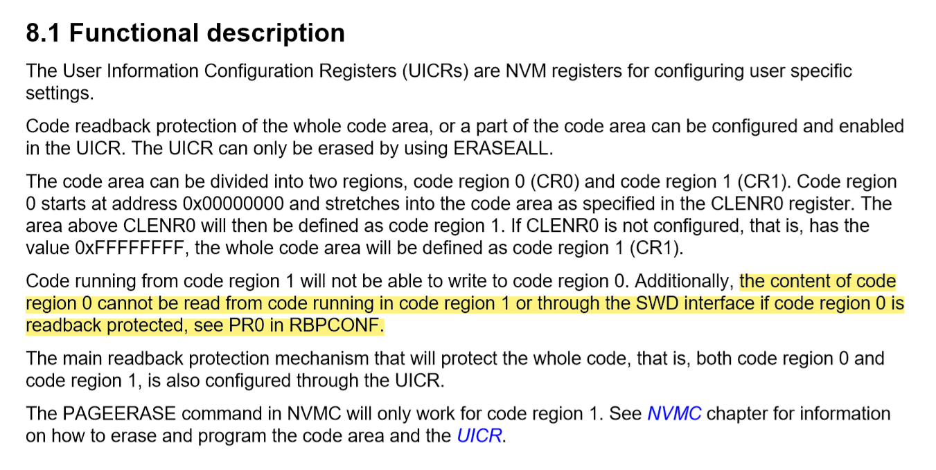
CR0标示代码地址不允许CR1部分代码或者调试口访问,该保护特性通过RBPCONF寄存器配置
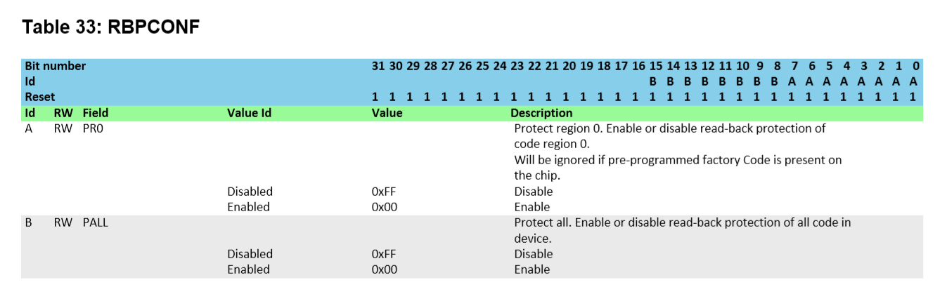
RBPCONF属于User Information Configuration Registers (UICR),这组寄存器配置了芯片的一些运行信息如bootloader地址,代码段长度等等
UICR必须写NVMC(Non-Volatile Memory Controller)的ERASEALL寄存器才能改,nvmc用来控制内存地址到flash的映射

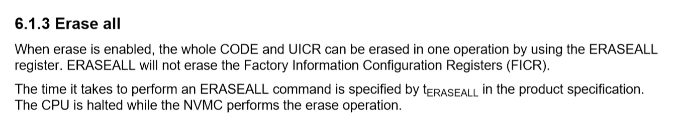
艹?必须要全擦除才行,等于UICR不能改,改了全部木大
是芯片的安全特性,不允许随便读写flash
0x2 利用pc读固件
看到了一篇文章 -> 传送门
大概思路是
- arm thumb指令长度是16bit,想要32bit寻址就只能通过寄存器寻址,不能直接在指令里面塞立即数
- readback保护是通过一个硬件模块实现的,只保护内存操作
也就是说可以随意操作寄存器的
改之前
改之后
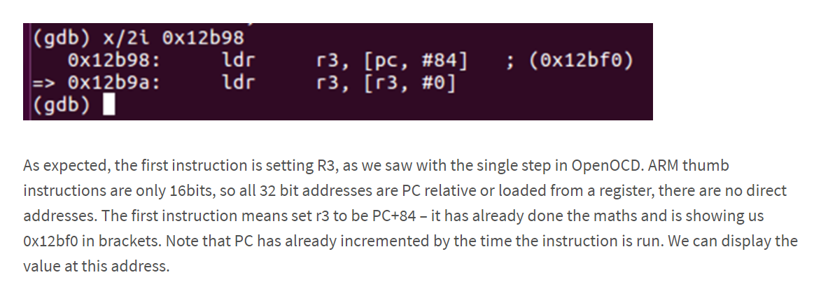
- 那么可以利用这句
LDR R3, [R3],R3可以是任意寄存器。只要猜出某个指令是直接用寄存器寻址,就操控pc一直跑那条指令,控制存地址的寄存器为要读取的内存地址
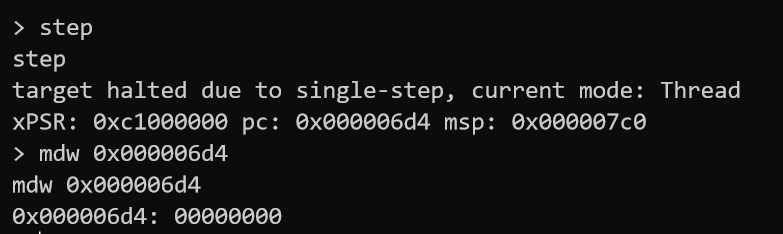
step过了几下,感觉我这个的R4拿来寻址了
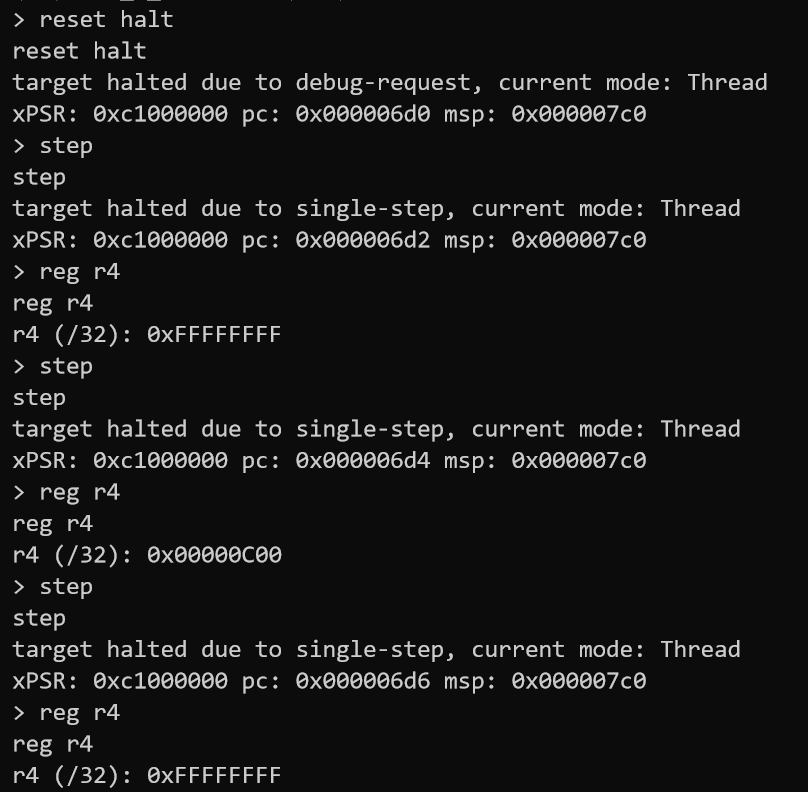
应该是0x6d4这个地址上的指令完成的寻址
把pc改过去试试,读一下RBPCONF配置
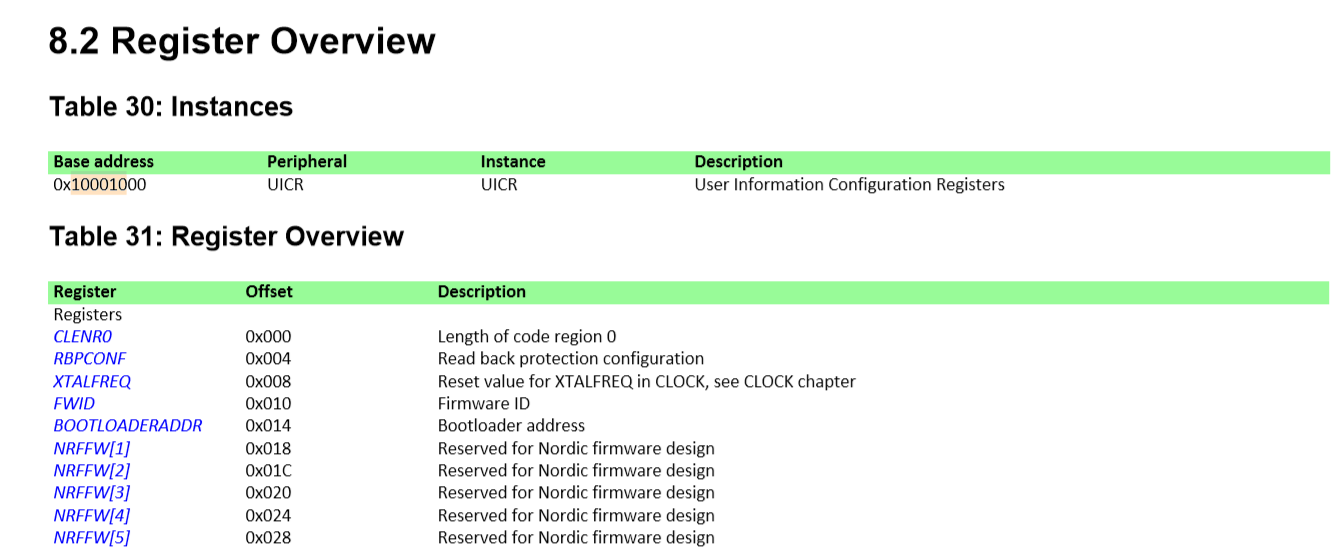
查了下手册在0x10001004上
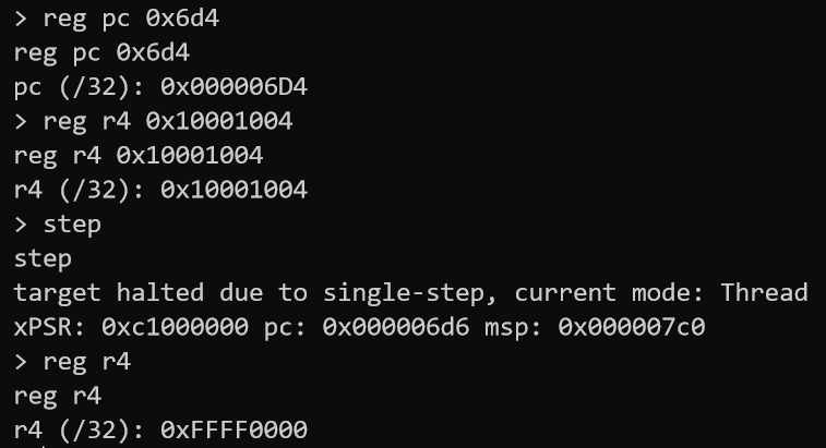
成功读出来是0xffff0000,保护全开
那么想要dump固件只需要重复执行这个过程把0x0-0x40000的数据读出来就行
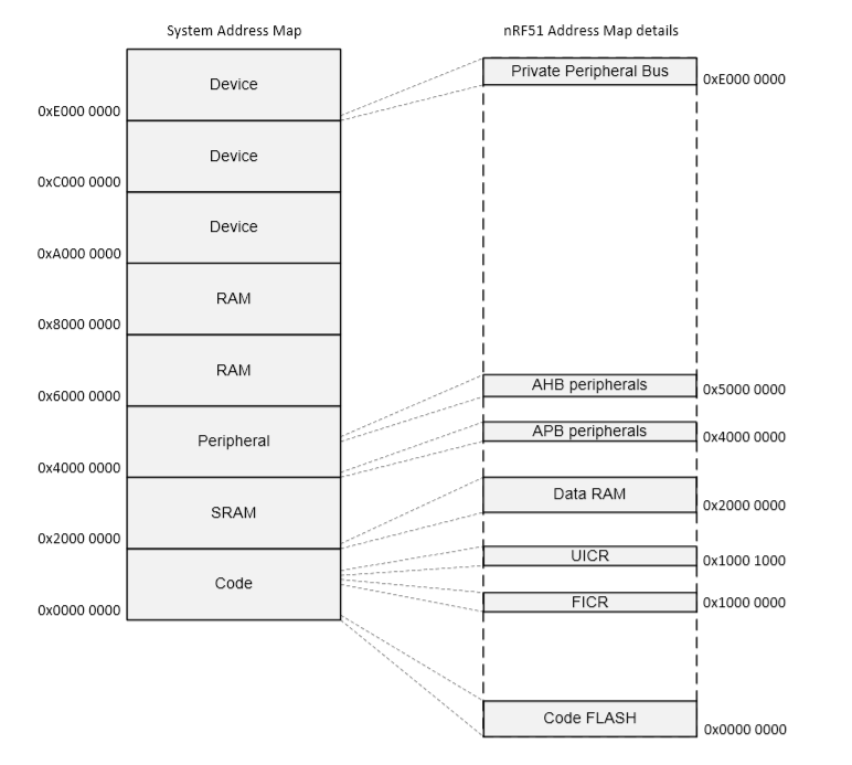
存在flash上的代码是直接映射到0x0的
0x3 dump固件
于是搓个脚本
from pwn import *
import re

p = remote("127.0.0.1", "4444")

p.recvuntil(">")
p.write("reset halt\n")
p.recvuntil(">")

with open("firmware.bin", "wb") as f:
    for addr in range(0, 0x40000, 4):
        p.write("reg pc 0x6d4\n")
        p.recvuntil(">")
        p.write("reg r4 " + hex(addr) + "\n")
        p.recvuntil(">")
        p.write("step\n")
        p.recvuntil(">")
        p.write("reg r4\n")

        ret = p.recvuntil(">")
        d = re.search('0x[0-9a-fA-F]{8}', ret.decode('utf-8'))[0]
        f.write(p32(int(d, 16)))
        if addr % 0x100 == 0:
            print("reading:", addr)
跑一下大概半个小时就读出来了,丢进ida看下
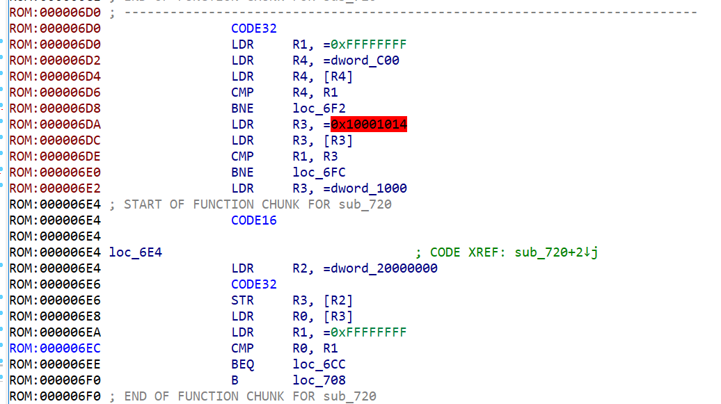
果然0x6d4是直接拿R4寻址
于是固件就成功提取了
彩蛋
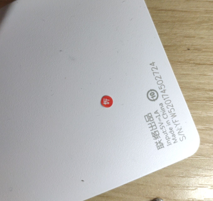
能被轻易完整取下的防拆标
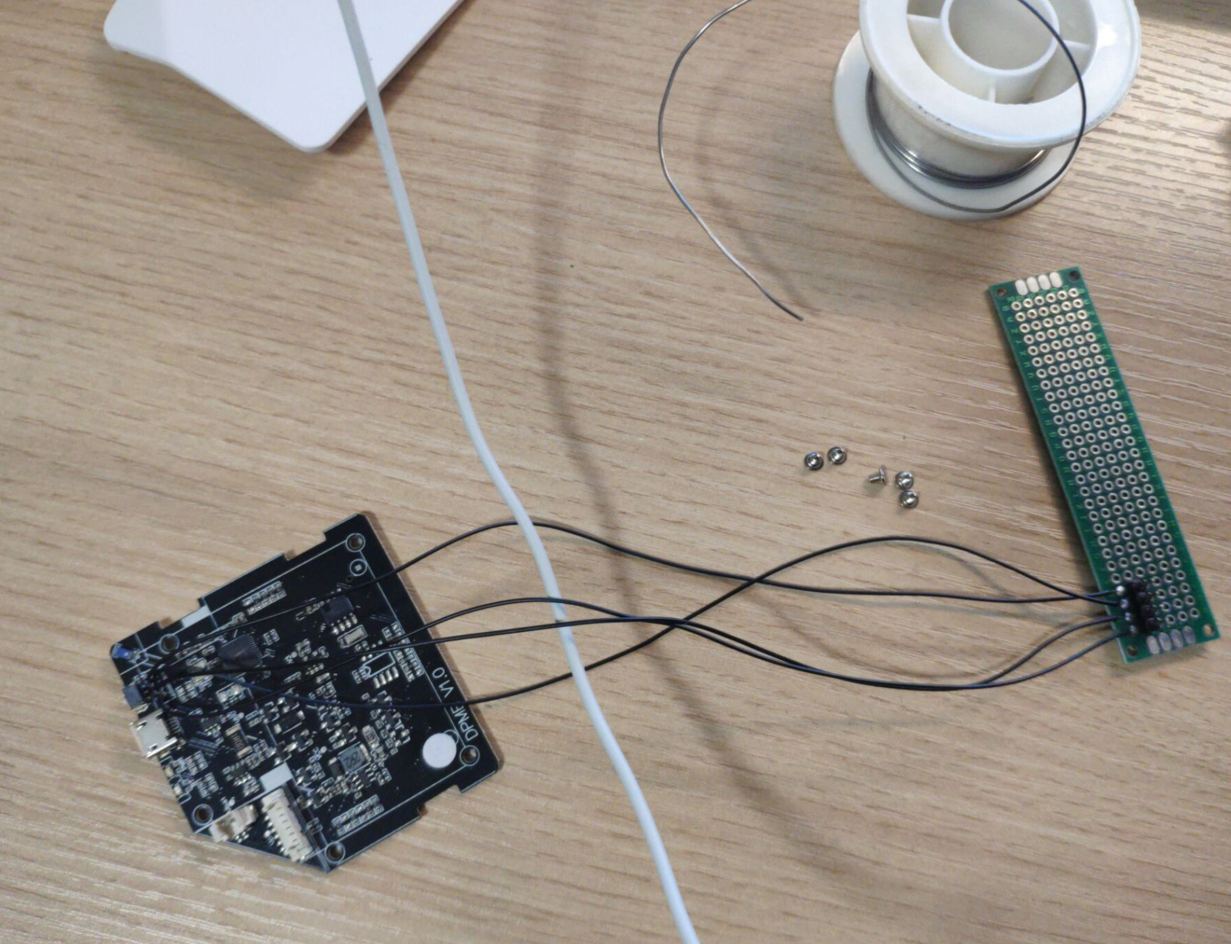
焊线不小心把耳机夹在了中间